EV Group, commonly called EVG, is a privately held semiconductor-equipment and process-technology company founded in 1980 by Aya Maria Thallner and engineer Erich Thallner. Its headquarters, product development and manufacturing remain in St. Florian am Inn, Austria. The company reports more than 1,700 employees worldwide, more than 1,300 of them at headquarters, with 30 locations and eight wholly owned subsidiaries.
EVG does not manufacture chips in Tempe. It makes and supports the specialized tools that semiconductor, MEMS, photonics and advanced-packaging manufacturers use to align, bond, pattern, coat, clean and inspect wafers and dies. Its main product families cover wafer bonding, optical and maskless lithography, nanoimprint lithography, resist processing, metrology and process-development services. The company says it holds the leading market position in wafer-bonding equipment and nanoimprint lithography. Those are company claims, not independently audited market-share figures.
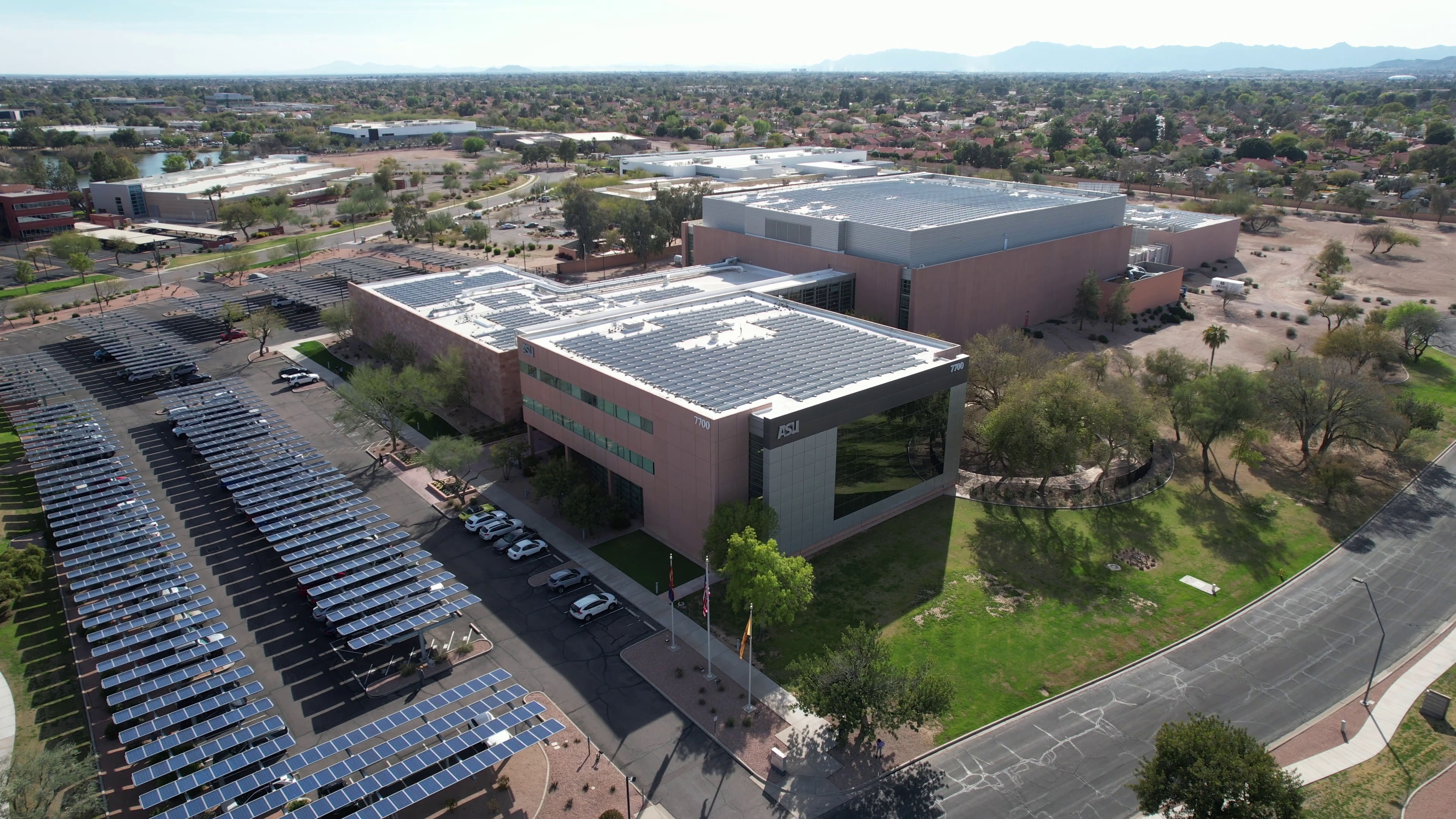
Arizona has been EVG's North American base since 1995. Its subsidiary, EV Group Inc., is at 7700 South River Parkway in the ASU Research Park in Tempe. EVG describes the location as a sales and technical-support center serving customers across North America. A 2004 expansion consolidated the subsidiary headquarters, Technology Center and customer support in Tempe and added a Class 10 cleanroom and laboratory for demonstrations, training and process development. The site therefore gives Arizona customers local engineering and service access, while EVG's manufacturing remains centralized in Austria.
EVG matters to AI because advanced computing is increasingly limited by how efficiently processors, memory and chiplets can be connected, not only by transistor design. EVG's wafer-to-wafer and die-to-wafer hybrid-bonding systems support dense three-dimensional integration, high-bandwidth memory and chiplet architectures. Its LITHOSCALE platform targets redistribution layers, interposers and fan-out packaging used in AI and high-performance computing. In May 2026, EVG and imec reported a 300 mm research test vehicle with 200 nanometer copper interconnect pitch and below 40 nanometer overlay across all measured dies. That was a research demonstration, not evidence of commercial production at that pitch.
The company's history is closely tied to technologies that moved MEMS and wafer bonding from laboratories toward volume manufacturing. EVG introduced a double-side mask aligner in 1985, separated wafer alignment from bonding in 1990, and launched a production wafer-bonding system in 1992. Later milestones include the SmartView alignment system, the GEMINI automated bonding platform, 300 mm production bonding, ComBond surface activation, LITHOSCALE maskless exposure and IR LayerRelease for thin-layer transfer.
EVG is also extending those integration methods beyond conventional chips. A 2021 partnership with ASMPT joined EVG wafer-bonding technology with high-precision die placement for die-to-wafer hybrid bonding. In 2026, EVG and Xanadu announced a partnership aimed at industrial-scale photonic quantum hardware. EVG also reported its fourteenth consecutive TechInsights Triple Crown in the 2026 customer-satisfaction survey. These awards and market-position statements help establish industry reach, but they originate from EVG and its cited survey partner.
Because EVG is private, public disclosures do not provide company revenue, Tempe headcount, Arizona payroll or a dollar value for the Tempe operation. ArizonaAI therefore does not estimate them. The verifiable Arizona story is narrower and still significant: EVG has maintained its North American base in Tempe for more than three decades and supplies local support and process capability for equipment used at critical fabrication and advanced-packaging steps.